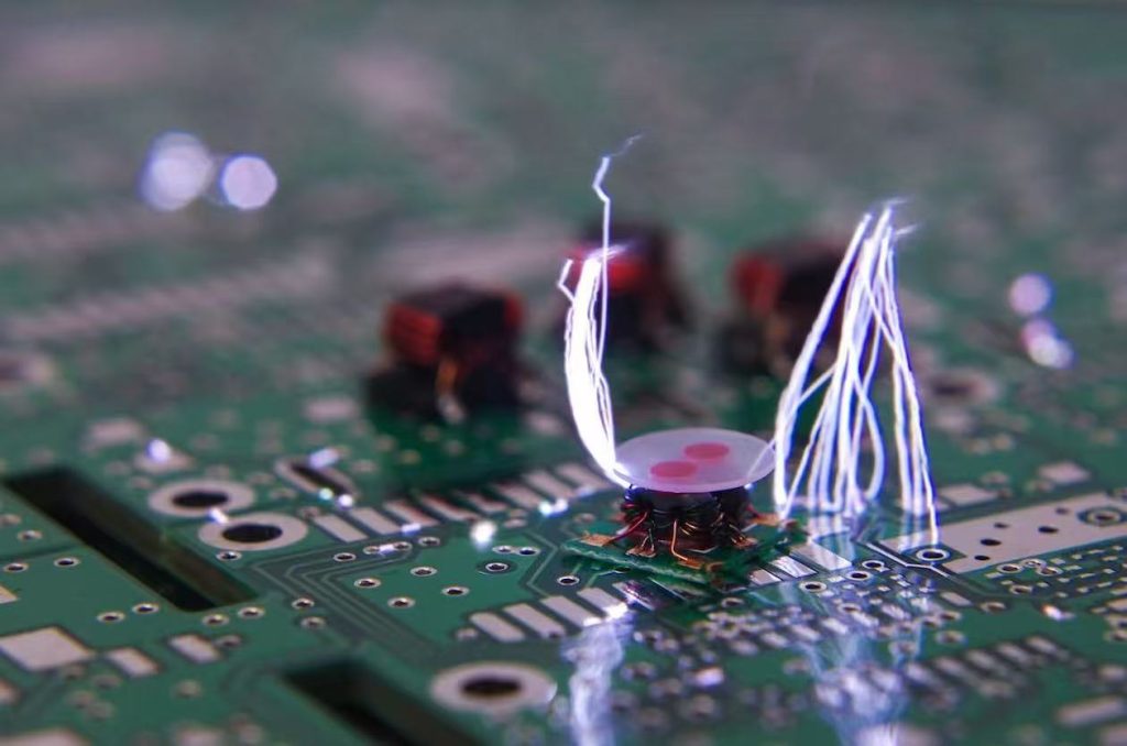
Electro-Static Discharge
Ever felt that sharp ‘zap’ when taking off a sweater in winter or touching a metal doorknob? That’s electrostatic discharge, or ESD.
For us, it’s a minor, momentary shock. But for today’s sophisticated electronics, it can be a catastrophic event. The internal circuitry of a microchip can be thousands of times thinner than a human hair. That same multi-thousand-volt ‘zap’ we feel can instantly puncture and destroy these delicate pathways, leading to device failure, system crashes, or permanent damage.
To ensure all electronic products operate reliably, they must pass strict ESD testing before release. This testing simulates real-world ESD events to verify if the device will malfunction, freeze, or be destroyed.
What is ESD Testing?
Simply put, ESD testing is a controlled stress test. Engineers use a specialized tool called an “ESD Gun” (or ESD Simulator) to mimic the discharge from a human body or another charged object. They apply these controlled zaps to a product’s enclosure, ports (like USB), and metal buttons to observe its reaction.
If the product continues to function normally, its protective design is adequate. If it crashes, reboots, or is damaged, the design is insufficient and must be revised by the engineering team.
Common ESD Standards
Different ESD scenarios require different standards. For example, the static generated by a factory worker handling a bare chip is vastly different from a user touching the outside of a finished product.
This leads to several layers of standards:
| Standard | Scope | Primary Application |
| IEC 61000-4-2 | System-Level | The global standard for all finished electronic equipment. Simulates a user touching the device. |
| ISO 10605 | System-Level | The specific standard for automotive electronics. It involves higher voltages (up to ±25kV) to simulate a driver/passenger. |
| HBM (Human Body Model) | Component-Level | A chip-level test that simulates a charged human touching a component’s pins during manufacturing. |
| CDM (Charged Device Model) | Component-Level | A chip-level test that simulates the chip itself becoming charged (e.g., sliding in a tube) and then discharging to a metal surface. |
Here’s a simple way to remember them: IEC for systems, ISO for auto, HBM/CDM for chips.
How is ESD Testing Performed?
The testing process is straightforward and typically involves three steps.
Step 1: Choose the Discharge Method
The ESD gun is applied to various points on the product.
- Contact Discharge: The gun’s metal tip directly touches a conductive part of the product (e.g., a screw, a connector shield). This is the preferred and most repeatable test method.
- Air Discharge: The gun is brought near an insulating part of the product (e.g., a plastic seam or button) until a spark jumps across the air gap.
Step 2: Set the Voltage Level
The test intensity is applied in steps. The most common standard, IEC 61000-4-2, defines these levels:
| Level | Contact Discharge | Air Discharge |
| Level 1 | ±2kV | ±2kV |
| Level 2 | ±4kV | ±4kV |
| Level 3 | ±6kV | ±8kV |
| Level 4 | ±8kV | ±15kV |
Step 3: Observe the Reaction
During the test, an engineer observes the Equipment Under Test (EUT). If it functions normally, the protection is excellent. If it glitches temporarily but self-recovers, it may still be acceptable. However, if it freezes, requires a manual reset, or is permanently damaged, the design has failed.
How Are Test Results Classified?
Based on international standards, the results are classified into four criteria:
| Criteria | Description |
| A | Pass: Normal operation, no impact. ✅ |
| B | Pass: Temporary glitch (e.g., screen flicker), but self-recovers with no loss of function. ✅ |
| C | Fail (Conditional): Temporary loss of function that requires manual intervention (e.g., a restart) to recover. ⚠️ |
| D | Fail (Hard): Permanent hardware damage or irreversible failure. ❌ |
A device that passes Level 4 (±8kV Contact, ±15kV Air) without reaching Criteria C or D is considered to be robustly protected.
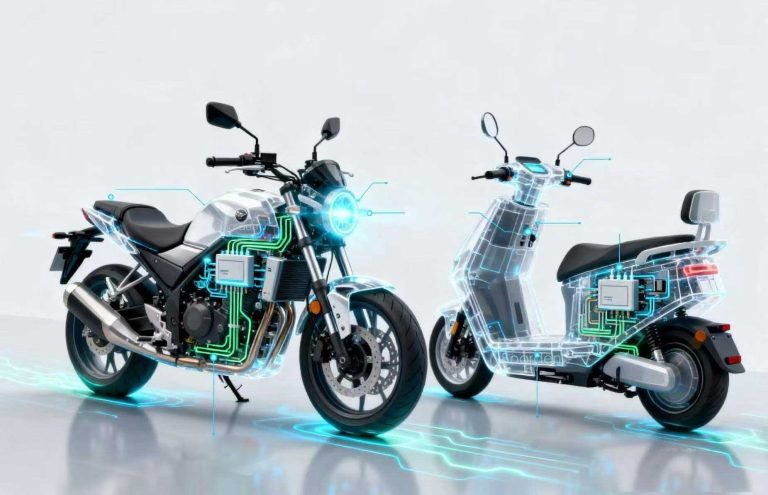
Why Are Automotive ESD Standards Stricter?
The automotive industry enforces much stricter ESD standards. ISO 10605, for instance, requires testing at various humidity levels and with discharge voltages as high as ±25kV.
This is because the automotive environment is electrically harsh. Static can build up from a driver sliding across a cloth seat, a technician servicing a wiring harness, or simply from the dry climate. A failure here is not just an inconvenience; it can be a safety risk.
Therefore, automotive electronics (infotainment systems, ECUs, lighting controllers, etc.) must be built with a much higher level of immunity.
How to Improve ESD Protection
To pass high-level ESD testing, protection must be “designed in” from the very beginning. This typically involves a three-pronged strategy.
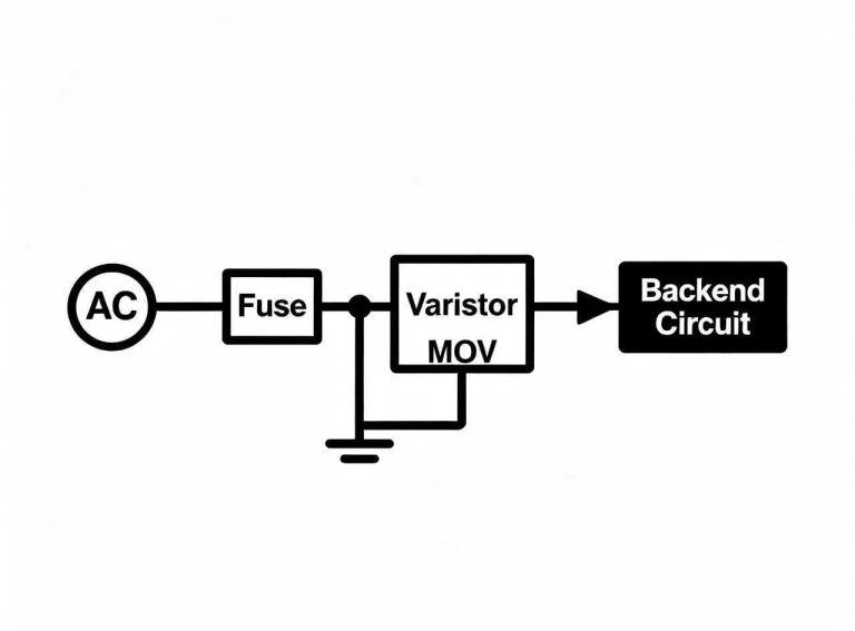
1. Add Protection Components
At vulnerable points like I/O ports and power inputs, engineers add components like SMD Varistors (MLVs) or TVS Diodes (Transient Voltage Suppressors). These components act like microscopic “shock absorbers,” activating in nanoseconds to absorb and divert the dangerous ESD energy away from the sensitive chip.
For example, Boarden’s CMSLDV series of multilayer surge-protection varistors are AEC-Q200 qualified and have passed IEC 61000-4-2 ESD testing. These components offer fast response and strong surge endurance, operating reliably in circuits with strict ESD and transient overvoltage requirements, such as in automotive electronics, telecom, and industrial control. In terms of design, ratings, and reliability, they serve as a perfect alternative to traditional automotive-grade varistors like the Panasonic ERZ series, providing clients with more flexible lead times and a superior cost-performance ratio.
2. Optimize PCB Layout
A good circuit board (PCB) layout is critical. Traces are kept short, and the ground plane is made solid and wide. This gives the ESD energy a clear, low-resistance path to follow, guiding it safely away from the sensitive ICs.
3. Implement Grounding & Shielding
A device’s enclosure is its first line of defense. A metal chassis must be properly grounded to the PCB, providing a safe path for the discharge. Plastic enclosures can be designed with internal shielding or insulating gaps to prevent the spark from ever reaching the internal electronics.
Summary
Electrostatic Discharge (ESD), while seemingly minor, is one of the most common “invisible killers” of electronic products. The purpose of ESD testing is to ensure a device can survive these real-world events, ultimately improving its reliability and lifespan.
By understanding these basic test methods and standards, you can better interpret a product’s test report (e.g., “Passes ±8kV Contact”) and appreciate why a truly “reliable” product always has dedicated protection components and thoughtful grounding design.
A device’s stability is often hidden in these tiny, critical details.
For more insights on circuit protection and ESD design, or if you’re facing specific ESD challenges in your projects, follow the Boarden Electronics LinkedIn. We are dedicated to the R&D and application of MOV, Varistor, TVS, and ESD protection devices. You can also connect with our engineering community (WeChat ID: 4027704) for practical case studies and technical resources.