
A 440 VAC and 4–6 kV Differential Surge Protection Solution for BLDC Motor Drivers
Keywords: BLDC motor driver, CMSL, high-energy SMD varistor, MOV, differential surge, residual voltage, clamping voltage, RCD, surge protection
Introduction
How Does Boarden CMSL Achieve High Input Voltage Tolerance with Lower Clamping Voltage?
For BLDC motor drivers designed to operate under high input voltage conditions while meeting stringent surge requirements, engineers often face a difficult trade-off: a higher-rated MOV can provide greater tolerance to high-line voltage, but may also result in higher residual voltage during a surge event.
This becomes particularly challenging in applications that need to withstand 440 VAC high-line operation and 4–6 kV differential surge tests.
A conventional solution may use two disc MOVs together with an RCD absorption network. While this approach can provide effective surge protection, increasing the MOV voltage rating may increase the clamping voltage seen by downstream components. Engineers may then need higher-voltage MOSFETs, capacitors, or other components to maintain sufficient safety margin.
The result can be a difficult balance between:
- High input voltage tolerance
- Low surge residual voltage
- MOSFET voltage rating
- Circuit cost
- PCB space
- Long-term reliability
- Manufacturing consistency
Boarden’s CMSL high-energy SMD varistor provides another approach: instead of requiring the front-end protection network to handle every protection task, the protection system can be divided into two stages.
The front-end MOV handles the major surge energy, while CMSL provides additional clamping at a critical downstream node.
A comparative test on a BLDC motor driver showed that the measured residual voltage under a 6 kV differential surge was reduced from 990 V to 744 V, a reduction of 246 V, or approximately 24.8%.
This article explains the protection concept, test results, and potential applications of this approach.
1. The Challenge: High Input Voltage vs. Low Surge Residual Voltage
A typical BLDC motor driver may include an AC input protection stage, EMI filter, bridge rectifier, DC bus, power MOSFETs, and motor control circuitry.
When a surge enters through the AC input, the front-end MOV absorbs and diverts part of the surge energy. However, the surge does not necessarily disappear after the first protection device operates.
A remaining transient can continue through the rectifier and DC bus toward downstream components.
For MOSFETs, electrolytic capacitors, gate drivers, and auxiliary power circuits, the important parameter is therefore not simply whether an MOV is installed at the input. What matters is how much voltage remains at the sensitive node after the surge passes through the entire protection path.
This creates a common design conflict.
If the MOV voltage rating is too low
The MOV may experience excessive leakage or unwanted conduction when the equipment operates at high input voltage.
For applications requiring 440 VAC high-line operation or high-voltage endurance testing, this may reduce the available design margin.
If the MOV voltage rating is increased
The higher-rated MOV can better tolerate the high input voltage, but its operating and clamping characteristics may also result in a higher voltage during a surge.
That higher residual voltage is then transferred to downstream components.
Engineers may compensate by selecting MOSFETs or capacitors with higher voltage ratings. While this can increase the electrical margin, it can also increase BOM cost and limit component selection.
For high-volume BLDC products, even a relatively small increase in component cost can become significant.
A more efficient protection strategy is therefore to separate energy absorption from voltage clamping.
2. Why Conventional MOV + RCD Protection Can Become Difficult to Optimize
2.1 Increasing the MOV Voltage Rating
Increasing the voltage rating of the front-end MOV can improve high-line operating margin.
However, this can also increase the voltage level during a surge.
In some designs, the resulting residual voltage may approach the voltage limit of downstream MOSFETs or other components. Engineers then have to select higher-voltage devices simply to compensate for the protection network’s residual voltage.
This approach can work, but it effectively transfers part of the protection burden to the power components.
For mass-produced products, this may lead to:
- Higher MOSFET cost
- Fewer available component options
- Larger voltage derating requirements
- Increased BOM cost
2.2 Using RCD or Larger Electrolytic Capacitors
Another common approach is to use an RCD network or a relatively large DC-bus capacitor to absorb part of the remaining transient energy.
This can be effective, but its performance may depend on several parameters, including:
- Capacitance
- ESR
- Component tolerance
- Temperature
- Aging
- Repetitive surge conditions
As these parameters change, the resulting transient voltage can also change.
For applications subjected to repeated surge events, electrolytic capacitors must additionally be evaluated for pulse charging stress, temperature rise, capacitance degradation, and long-term reliability.
Simply increasing capacitance is therefore not always the most efficient solution. It can increase component size, cost, and PCB area while introducing additional design considerations.
2.3 Adding More Protection Components
Another option is to add additional MOVs, RCD networks, capacitors, or other discrete protection stages.
Multiple protection stages can distribute the surge energy, but they also introduce a new engineering challenge:
How should the protection stages coordinate with each other?
Engineers need to consider:
- Which device conducts first?
- How much energy does each stage absorb?
- Is there sufficient voltage coordination between stages?
- How short is the high-di/dt current path?
- How do component tolerances affect protection?
- Will the protection relationship remain stable after aging?
More protection components do not automatically mean better protection.
For compact BLDC control boards, additional components also increase PCB congestion and make layout and debugging more complicated.
3. CMSL: Front-End Energy Absorption + Downstream Clamping
Boarden CMSL is a high-energy SMD varistor designed for surge protection applications where both energy handling and compact PCB implementation are important.
Like conventional MOVs, a varistor normally remains in a high-resistance state during normal operation. When a transient surge occurs, it rapidly changes to a low-resistance state, diverting surge current and limiting the voltage at the protected node.
The key difference in the application described here is not that CMSL replaces every front-end protection component.
Instead, the protection system is divided into two functions:
The front-end MOV handles the major surge energy, while CMSL provides additional clamping at a critical downstream node.
This allows the protection network to address two different requirements independently:
Stage 1 — Energy absorption
The front-end MOV provides the primary surge current path and handles the major portion of the surge energy.
Stage 2 — Voltage clamping
CMSL is positioned closer to the sensitive downstream circuit to further limit the transient voltage reaching critical components.
This approach can be particularly useful when the front-end MOV cannot simultaneously provide sufficient high-line tolerance and sufficiently low residual voltage.
4. BLDC Motor Driver Comparison
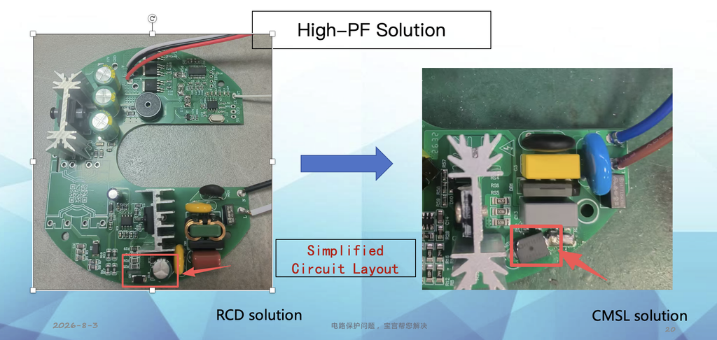
A high-power BLDC motor driver was evaluated using two protection configurations.
| Protection Item | Conventional Solution | CMSL Solution |
|---|---|---|
| Front-end protection | 2 × 14D621 MOV | 1 × 14D621 MOV |
| Additional protection | RCD | CMS3025V681P401-L05FD |
| Protection concept | MOV limiting + RCD absorption | Front-end energy absorption + downstream clamping |
| Main design considerations | Capacitance, ESR, tolerance, aging | Protection coordination, energy distribution, PCB layout |
The CMSL solution does not simply remove the primary surge protection stage.
Instead, the front-end MOV continues to provide the main surge-energy path, while the CMSL device performs additional voltage clamping at the downstream protection node.
This division of responsibilities is the key to the design approach.
5. 6 kV Differential Surge Test: 990 V vs. 744 V
The most important result of the comparison was obtained under a 6 kV differential surge test.
The same test board, test wiring, surge generator conditions, and measurement point were used to compare the two protection configurations.
| Protection Solution | 6 kV Differential Surge Residual Voltage | Result |
|---|---|---|
| 2 × 14D621 + RCD | 990 V | Baseline |
| 1 × 14D621 + CMS3025V681P401-L05FD | 744 V | 246 V lower |
The CMSL configuration reduced the measured residual voltage from 990 V to 744 V.
That represents a reduction of approximately:
246 V / 990 V ≈ 24.8%
Why does the 246 V reduction matter?
A lower residual voltage can provide additional transient voltage margin for downstream components such as:
- Power MOSFETs
- DC-bus capacitors
- Gate-driver circuits
- Auxiliary power supplies
- Other sensitive semiconductor devices
The result may also create an opportunity to reassess the voltage rating and cost of downstream components.
However, a lower measured residual voltage does not automatically mean that a lower-voltage component can be substituted.
The final component selection must still be verified against the complete circuit, operating conditions, required derating, surge waveform, repetition count, and applicable product-level testing.
6. Why SMD Implementation Matters
The electrical performance of a surge protection device is only one part of the design.
For compact BLDC motor drivers, PCB layout and manufacturing also matter.
Compared with traditional leaded disc components, an SMD solution can provide several potential system-level advantages.
6.1 More Flexible PCB Layout
The smaller SMD footprint can make it easier to position the protection device close to the protected node.
This is especially important for high di/dt surge currents, where parasitic inductance in PCB traces and component leads can affect the voltage observed at the protected circuit.
A shorter surge-current path can help reduce unwanted parasitic voltage.
6.2 SMT Manufacturing Compatibility
CMSL can be integrated into automated SMT assembly processes, reducing the need for separate through-hole assembly operations.
For high-volume production, this can simplify manufacturing flow and improve production efficiency.
6.3 Compact Protection Architecture
Replacing a larger combination of discrete protection components with a carefully evaluated SMD protection device can help free PCB space.
This is particularly relevant to compact BLDC control boards where component density continues to increase.
However, PCB layout remains critical. The protection device should be positioned according to the actual surge-current path rather than simply placed near the protected component.
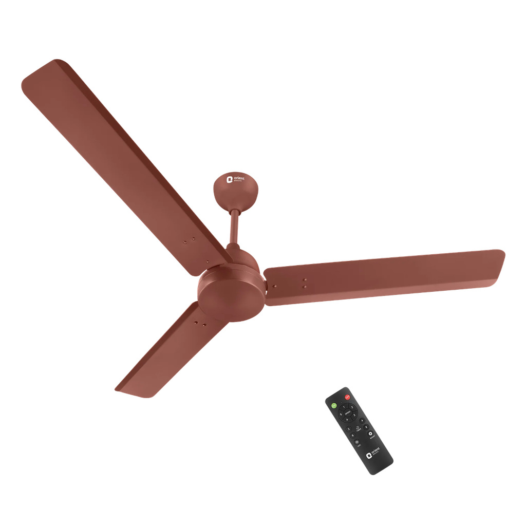
7. Applications Beyond BLDC Ceiling Fans
The high-input-voltage and low-residual-voltage conflict is not limited to ceiling-fan motor drivers.
The same protection concept may be worth evaluating in other applications where a high-energy front-end surge must be combined with tighter downstream voltage control.
7.1 Low-Power BLDC Motor Drivers
Low-power BLDC applications may rely on DC-bus capacitors to absorb part of the transient energy.
When surge levels increase or repeated surge events become part of the product requirement, the capacitor may experience additional electrical and thermal stress.
Depending on the circuit, system voltage, surge level, available PCB space, and energy requirements, CMSL devices such as CMS1206V561P101 or CMS3025V561P401-L05FB may be evaluated as part of a compact secondary protection strategy.
The final device selection should always be determined by the actual circuit and product-level test results.
7.2 Blowers and Industrial Fans
BLDC blowers and industrial fans share many characteristics with ceiling-fan motor drivers:
- AC input
- Rectification
- DC bus
- Power MOSFETs
- Motor control circuitry
- Exposure to power-line transients
Longer cables and more variable field environments can further increase the importance of surge protection.
As power levels increase, the design objective may shift from simply asking:
Can the circuit pass the surge test?
to:
How low can the residual voltage be while maintaining sufficient energy-handling capability?
This is where a coordinated front-end MOV and downstream CMSL protection strategy may provide an alternative design path.
7.3 Other Power Electronics Applications
The same concept may also be evaluated in:
- LED drivers
- Switching power supplies
- Smart-home control boards
- Appliance control boards
- Power conversion equipment
- Industrial control electronics
In these applications, engineers may face the same fundamental trade-off:
The input stage needs to tolerate a wide or high operating voltage range, while downstream semiconductors require a lower transient voltage.
Instead of continuously increasing the voltage rating of downstream components or adding more absorption components, engineers can evaluate whether a two-stage protection architecture can better distribute the protection responsibilities.
8. How Should Engineers Evaluate a CMSL Solution?
CMSL should not be considered a universal replacement for an entire surge protection network.
High-energy surge protection is a system-level problem involving:
- Surge source
- Input voltage
- MOV characteristics
- Circuit impedance
- Fuse
- PCB copper
- Wiring inductance
- Protected-node location
- Downstream component ratings
A practical evaluation should therefore compare the existing solution and the CMSL solution under identical conditions.
At minimum, engineers should evaluate:
- Normal operating voltage and maximum input voltage
- Required surge voltage and current
- Differential-mode or common-mode surge conditions
- Surge waveform and repetition count
- Measured residual voltage at the actual protection node
- Energy distribution between protection devices
- MOSFET and capacitor voltage margin
- PCB surge-current path and parasitic inductance
- Component tolerance and temperature
- Post-surge leakage and product-level reliability
For products targeting markets with unstable or highly variable power grids, such as parts of India and Southeast Asia, the protection design should also consider the actual operating environment rather than relying only on nominal input voltage.
Conclusion: Surge Protection Is More Than Passing the Test
For BLDC motor drivers, passing a surge test once is not necessarily the final objective.
A robust protection design needs to balance:
- High-line operating voltage
- Surge residual voltage
- MOSFET voltage rating
- Repetitive surge capability
- Component aging
- PCB space
- Manufacturing consistency
- Total BOM cost
When a design must withstand 440 VAC high-line conditions while also meeting 4–6 kV surge requirements, simply increasing the MOV voltage rating or adding more absorption components may not always be the most efficient approach.
A coordinated architecture can instead assign different protection tasks to different stages:
The front-end MOV handles the major surge energy, while the CMSL high-energy SMD varistor provides additional clamping at a critical downstream node.
In the BLDC motor-driver comparison presented here, this approach reduced the measured residual voltage under a 6 kV differential surge from 990 V to 744 V — a reduction of 246 V, or approximately 24.8%.
The value of this reduction is not limited to one ceiling-fan application. It provides additional voltage margin for downstream components and creates an opportunity to reconsider component ratings, PCB layout, protection architecture, and BOM cost.
For engineers facing the combination of 440 VAC operation, 4–6 kV surge protection, high MOSFET voltage ratings, and limited PCB space, CMSL is worth evaluating as part of a coordinated two-stage surge protection strategy.
Technical Inquiry
If you are developing a BLDC motor driver or other power electronics application and need to evaluate a high-energy SMD varistor, please share your:
- Input voltage range
- Surge test level
- Existing MOV/RCD configuration
- Target residual or clamping voltage
- Protected component voltage rating
- PCB space limitations
The Boarden engineering team can evaluate a suitable CMSL configuration based on your application requirements and test conditions.