Understanding the Three Major ESD Models (HBM/CDM/MM) and Their Protection Design Strategies
In modern electronic systems, Electrostatic Discharge (ESD) is one of the most common — and destructive — electrical threats. It can occur during manufacturing, transportation, assembly, or even during routine use. In mild cases, ESD may cause temporary malfunction; in severe cases, it can lead to permanent device damage.
To evaluate the ESD robustness of electronic components during development and production, the industry widely uses three standardized models:
- HBM (Human Body Model)
- CDM (Charged Device Model)
- MM (Machine Model)
Each model reflects a different ESD event, with unique discharge characteristics, testing standards, and applicable scenarios. This article offers an in-depth comparison of the three models, explores their significance in ESD design, and provides practical protection strategies — along with Boarden’s recommended circuit protection solutions.
What is ESD?
Electrostatic Discharge (ESD) is a sudden flow of electric current caused by the transfer of charge between objects at different potentials. ESD events can easily reach several thousand volts and frequently occur when:
- Operators handle tools or touch components
- Devices are moved or packaged
- PCBs are assembled or inspected
ESD can damage sensitive components such as LED drivers, ICs, and communication interfaces. Typical consequences include:
- Destruction of semiconductor junctions
- Signal transmission errors or data loss
- Reduced lifespan and long-term reliability of devices
Understanding ESD models is essential for building effective protection strategies in electronic design.
Overview of the Three ESD Models
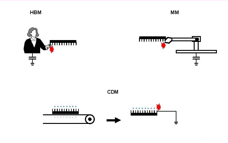
Human Body Model–HBM
- Concept: Simulates ESD from a charged human body touching a component. The test circuit uses a 100pF capacitor and 1.5kΩ resistor to discharge.
- Standard: ANSI/ESDA‑JEDEC JS‑001 (formerly JESD22-A114 / STM5.1)
- Characteristics:
- Discharge duration: 2–10 ns
- Peak current: ~0.67 A/kV
- Commonly used to assess risks during handling and assembly
- Use Case: Evaluates susceptibility to human contact during production.
Charged Device Model–CDM
- Concept: Simulates a component itself being charged and then suddenly discharging upon contacting a grounded conductor.
- Standard: ANSI/ESDA‑JEDEC JS‑002 (replaces JESD22-C101 / STM5.3.1)
- Characteristics:
- Ultra-fast discharge: <1 ns rise time
- Peak current: tens of amps
- Represents the most common and severe ESD risk in automated assembly lines
- Use Case: Especially critical for SMD components on high-speed pick-and-place machines.
Machine Model–MM
- Concept: Simulates discharge from a charged machine or tool making contact with a component. Test setup typically uses a 200pF capacitor and negligible resistance.
- Standard: ESD STM5.2 / JESD22-A115
- Characteristics:
- High-energy discharge similar to a low-impedance spark
- Less repeatable and mostly obsolete in modern testing
- Use Case: Historical reference; rarely used in current industry standards.
ESD Model Comparison Table
| Model | Capacitance | Resistance | Discharge Duration | Peak Current/Voltage | Real-World Scenario |
|---|---|---|---|---|---|
| HBM | 100 pF | 1.5 kΩ | 2–10 ns | ~0.67 A/kV | Human touch ESD during production |
| CDM | ~4–30 pF | ~0 Ω | <1 ns | Tens of amps | Component discharges to ground in automated lines |
| MM | 200 pF | ≈0 Ω | ~5–8 ns | High voltage pulse | Machine/tool contact discharge (mostly outdated) |
✅ Summary:
- CDM has the highest discharge speed and peak current — most dangerous to chips.
- HBM covers the most common human handling risk.
- MM is largely historical and less relevant today.
Core Design Strategies for ESD Protection
To address the characteristics of each model, consider the following design practices:
- 1. TVS Diodes (Transient Voltage Suppression)
- Ultra-fast response, capable of clamping voltage spikes within nanoseconds
- Highly effective against both HBM and CDM
- Should be placed as close as possible to the sensitive IC
- 2. Low-Capacitance ESD Arrays for High-Speed Interfaces
- Ideal for USB, HDMI, Type-C, and other differential high-speed signals
- Use DFN or other compact, low-cap packages to preserve signal integrity
- 3. PCB Layout and Ground Optimization
- Minimize trace length between protection device and IC
- Add damping resistors or RC filters where necessary
- Improve ground return paths to reduce CDM discharge paths
- 4. ESD Control in Production Environment
- Ensure operator wrist straps and work surfaces are grounded
- Maintain appropriate humidity and use ionizing fans to reduce static buildup
- Implement HBM/CDM-based component sensitivity classification and tracking
Boarden’s ESD Protection Product Recommendations
Based on the above design strategies, Boarden offers tailored solutions to meet ESD protection needs across multiple applications:
| Product Category | Package | Features | Typical Application |
|---|---|---|---|
| TVS Diode Series | SOD-323, SOT-23 | Fast clamping, wide voltage range | LED drivers, power inputs |
| Low-Cap ESD Arrays | DFN, SOT-363 | Suitable for high-speed signals | USB, HDMI, Type-C interfaces |
| CMS SMD Varistors | 0603–2220 | High surge capability, low clamping voltage | AC inputs, industrial power lines |
| BIS Common Mode Suppressors | Custom patent design | Combines ESD & surge suppression | Lighting, communication, EV chargers |
📌 If you’re interested in samples or application-specific guidance, contact Boarden team can help you identify the most suitable part numbers based on your circuit requirements.
Understanding the principles behind HBM, CDM, and MM models is critical to building robust, compliant electronics. By combining CDM-sensitive testing with HBM-based design strategies, engineers and quality teams can ensure protection across the entire product lifecycle — from assembly to deployment.
With over a decade of experience in circuit protection, Boarden Electronics offers complete solutions — from component selection to PCB layout guidance and pre-compliance verification.